Energy Harvesting SoC
Overview
 As part of a research group working on a lab on a chip system, I implemented a reconfigurable metal array using MOSFETS,
poly resistors, and MiM capacitors to allow small arbitrary analog and digital systems to be laid out post tapeout. This is
done using laser etching with gold on the highest metal layer. It features small arrays that can be laid out
as space permits and has been designed to allow easy routing, given the restrictive sizes of traces required. For the etching,
the metal runs have to be at least 2um wide and have 2um of space between eachother. It has been taped out in Skywater 130nm. Below is a sample
circuit using the array.
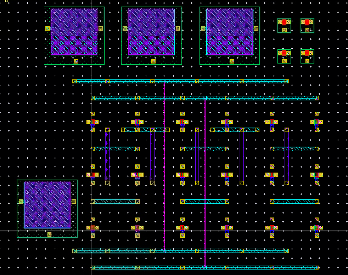
As part of a research group working on a lab on a chip system, I implemented a reconfigurable metal array using MOSFETS,
poly resistors, and MiM capacitors to allow small arbitrary analog and digital systems to be laid out post tapeout. This is
done using laser etching with gold on the highest metal layer. It features small arrays that can be laid out
as space permits and has been designed to allow easy routing, given the restrictive sizes of traces required. For the etching,
the metal runs have to be at least 2um wide and have 2um of space between eachother. It has been taped out in Skywater 130nm. Below is a sample
circuit using the array.
